- Home
- >
- News
- >
- Industry news
- >
- figuring out the details of your pcb’s stackup
figuring out the details of your pcb’s stackup
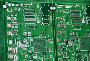
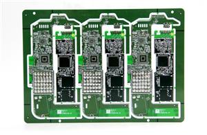
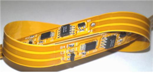
Making sure your board has the right number of layers, with the correct thickness and material type, and in the proper orientation can sometimes be an entire job in itself. Not to mention the complexity of creating multiple layer stacks, each with their own set of constraints. Stackups for flexible board regions have their own set of unique requirements for things like coverlay, stiffeners, surface coating and core materials. Managing all of this in an organized way can be a difficult task.
Bending and fitting your board into a mechanical housing without spending money to build a prototype, is a difficult task when designing rigid-flex. Component bodies on different sections of the device may interact in ways you didn’t expect, or dimensions of flexible sections may not be designed properly to bend like you want. How can you design such a dynamic, physical object without actually being able to hold it in your hands?
Prototyping is essential when you’re designing flexible electronics, but it doesn’t mean a whole lot if you can’t accurately convey your design intent to a manufacturer. When it comes to rigid-flex design, standard documentation usually isn’t enough to do that, and there are unique elements you need to specify directly to your manufacturer. What’s the best way to make sure your manufacturer follows your stackup guidelines and specifications? How do you accurately show how your board bends and folds?