- Home
- >
- News
- >
- Industry news
- >
- What is the PCB test point?
What is the PCB test point?
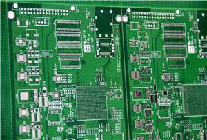
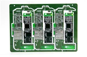
The parts on the PCB are complex and diverse. Are all these parts in accordance with the specifications?Can all be soldered?If it does not meet the requirements of the process, it is not allowed to be manufactured, otherwise it cannot be used.Therefore, it is very important to test before manufacturing, which requires the PCB test point.The so-called PCB test point is used to test whether the zero device on the circuit board conforms to the specification and weldability.
Measurement Of PCB, generally using ICT(in-circuit -Test), or automated testing machine, is used to Test all parts Of the board that need to be measured by Bed-Of Nails.The speed of the test machine is generally very fast, but when the probe touches the part or the foot, it may crush it, so that the unproblematic device becomes problematic.
To solve this problem, there is a "test point", in the ends of the additional parts to elicit a pair of round dots, there is no welding (mask), can make a test probe access to these small points, without direct access to those measurement of electronic parts, so you don't have to worry about parts are damaged.
Knowing the importance of test points, what are the process requirements for making test points?*** talk to everyone:
1. The welding disc used for welding zero parts shall not be used as the test point, and special test welding plates shall be designed separately.The welding disc is in the same side of PCB, so it is easy to detect and reduce the corresponding cost.
2. The test points shall be made of metal with soft texture, easy to penetrate and not easy to oxidize, so as to ensure a reliable grounding and prolong the service life of the probe.3. The test point should be greater than 5mm from the edge of PCB;It should be placed around 1mm around the element to avoid impact of probe and element.It needs to be placed around 3.2mm around the annular ring.
4. The diameter of test point is not less than 0.4mm, and the distance between adjacent test points is better than 2.54mm, but not less than 1.27mm.
5. The test points should be evenly distributed on the PCB to reduce the pressure concentration of the probe;The power supply line should be set up in the PCB to test the breakpoint so that the power can be connected or the fault point is checked.