- Home
- >
- News
- >
- Industry news
- >
- What is Via in pad technology?
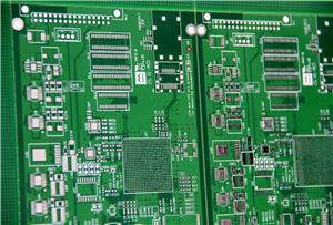
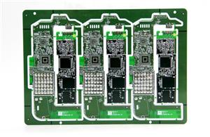
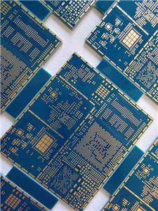
What is Via in pad technology?
1. plug via by solder mask.
This solution is suitable for big solder SMD pads, no cost addition.
The standard LPI solder mask process cannot tent of fill vias without the risk of
exposed copper inside the hole barrel. typically,a secondary screen print operation is used that deposits uv or thermally curable epoxy soldermask into the holes to plug them.
This is called via plugging. Via plugging is used to plug via holes with a solerrsist material to prevent air leakage during in circuit test, or to prevent shortin from
Components that are close to the board surface
2. Plug the via by resin and plated it flat by copper.
It is suitable for small BGA via in pad.
This process fill the via hole with a conductive or nonconductive material and then the via surface is plated over to provide a smooth flat solderable surface. there are used for
Via-in-pad designs where component may e mounted over the via,or a solder joint will extend
over the via connection.
3. Microvias and via in pad plated over.
According to IPC,a microvia is a hole with a diameter of < 0.15mm.
It can be a through viahole (with all respect to a aspect ratio),
But we normally see them as blind vias between 2 layers.
Mostly drilled by laser,but some pcb manufactuers are also drilling mircorvias with a mechanical drill bit. it is slower,but the holes have a clean and nice cut.
The microvia copper fill process is an electrochemical depossition process applied in the manufacturing of multilayer process,also called capped vias.
The process is complex,copper filling of microvias is available from most manufacturers
That are capable of producing HDI PCB Boards.