

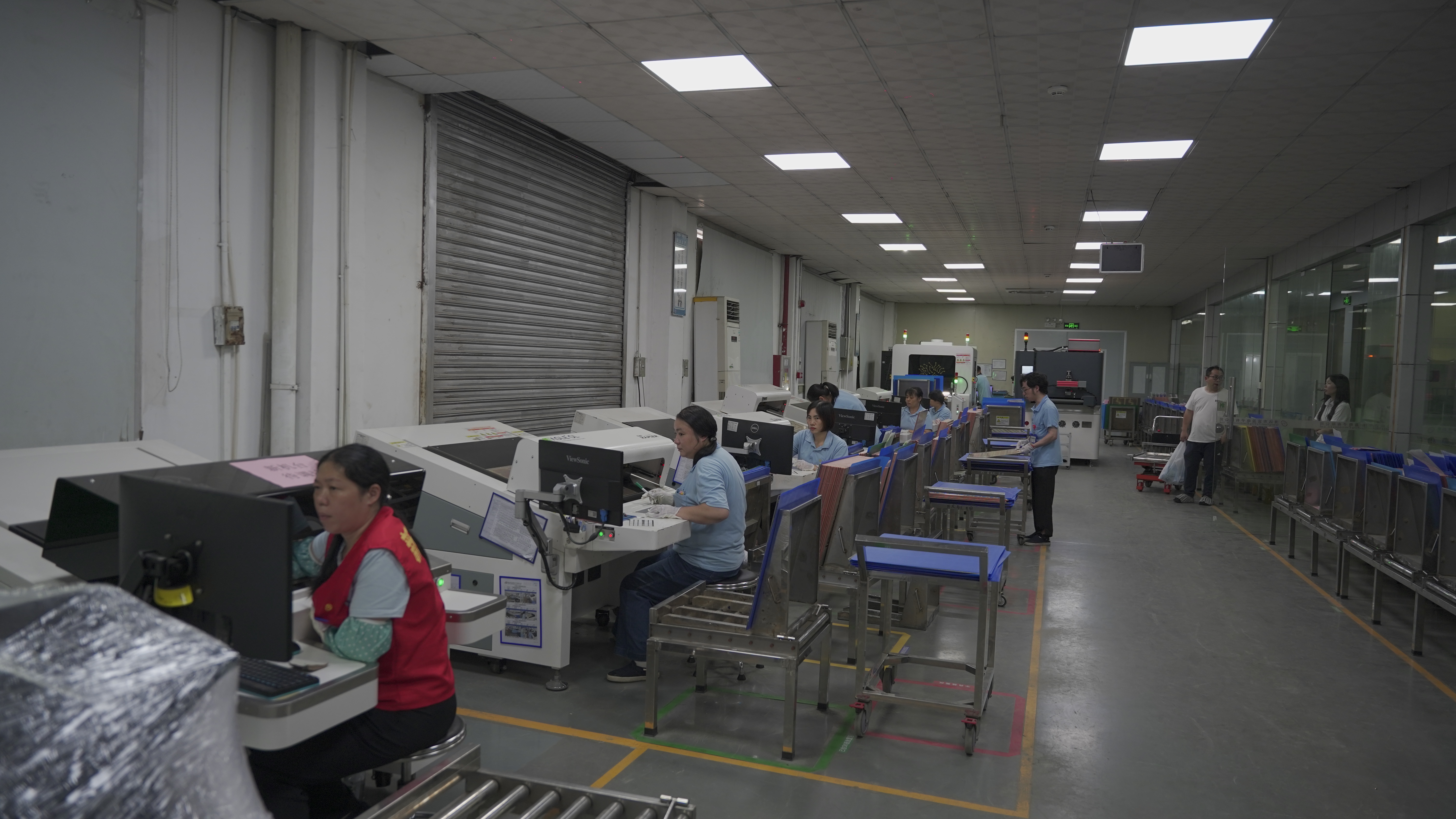
AOI Inspection
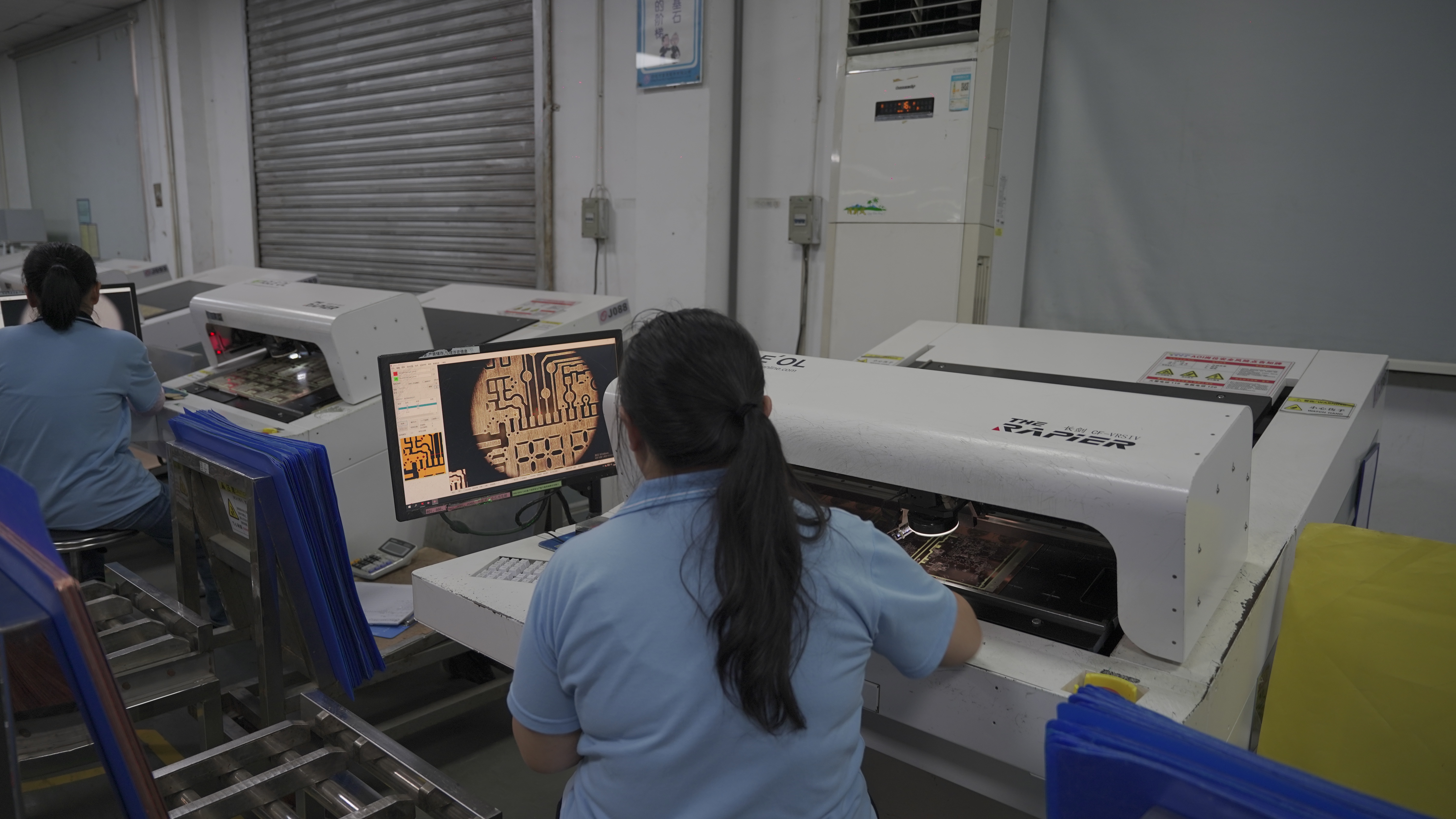
AOI Inspection
PCB Inner & Outer Layer AOI Automatic Optical Inspection Machine
Product Overview
Core Advantages
Dual Models for Inner & Outer Layer Professional Inspection: Targeted optimized algorithms for inner layer and outer layer processes respectively. The inner layer AOI accurately judges open circuits, short circuits, line gaps and copper residue before lamination, avoiding batch defective lamination waste. The outer layer AOI comprehensively inspects finished circuit flaws such as line distortion, pinholes, scratches and oxidation defects, achieving full-process quality control.
High-precision AI Intelligent Recognition: Equipped with ultra-high-definition industrial camera and multi-angle light source system, it supports micron-level defect capture. The self-learning AI algorithm effectively filters false defects, greatly improving detection accuracy and stability. It can stably identify ultra-fine line defects of high-density HDI boards, ensuring zero missed detection of key quality risks.
High Efficiency & Cost Saving: Fully automatic scanning and intelligent detection replace traditional manual visual inspection. The machine features fast scanning speed and large single-panel detection range, which greatly improves production inspection efficiency and reduces labor costs. It effectively avoids quality complaints and rework losses caused by human missed detection, realizing overall production cost reduction.
Powerful Compatibility for Various PCB Types: Adaptable to various board thicknesses, copper thicknesses and special substrate materials, including ultra-thin core inner layers, thick copper outer layers, high-frequency materials and aluminum substrates. It supports inspection requirements from small-batch prototype proofing to large-scale mass production with strong production flexibility.
Intelligent Data Recording & Traceability: The equipment automatically saves inspection data, defect images and statistical reports, realizing full-process quality traceability. It helps the production team optimize front-end processes, reduce repeated defects, and continuously improve PCB production yield and quality stability.
Technical Parameters
Equipment Type: Inner Layer AOI Inspection Machine / Outer Layer AOI Inspection Machine
Minimum Detectable Defect: 0.01mm micron-level tiny flaw
Inspection Accuracy: ≥99.8% recognition rate, ultra-low false detection rate
Applicable Board Thickness: 0.05mm – 6.0mm
Applicable Line Width Range: Ultra-fine line 0.03mm and above
Compatible Board Types: Multi-layer PCB, HDI high-density board, heavy copper PCB, ultra-thin core board, high-frequency PCB
Working Mode: Fully automatic feeding, scanning, identification and data recording
Data Function: Automatic defect classification, report export, full quality traceability