
ENIG Ceramic Base PCB
- Multech
- China
- 10-15 days
- 88000sqm/month
Product Description:
The Ceramic Base PCB with Superior thermal conductivity is a type of board that uses a ceramic base (Al₂O₃, AlN, or BeO) instead of the organic materials normally used. This high thermal conductivity board (>170 W/m·K for AlN) can match the very low coefficient of thermal expansion (CTE) of silicon chips and, using thin-film or thick-film metallization processes it also enables high-frequency performance. Ceramic PCBs are the best choice for applications such as high power LEDs, laser diodes, RF power amplifiers, and hybrid microelectronic circuits, where the ability to withstand extreme temperature changes is a requirement for reliability.
Product Specifications: ENIG Ceramic Base PCB
Parameter Category | Specification |
|---|---|
Board Thickness | 1.0mm |
PCB Type | Ceramic Base |
Line Width/Space | 4/4mil |
Surface Finish | ENIG (1U”) |
Finished Copper Thickness | 2oz |
Testing Standard | 100% AOI Test |
Certifications | ISO 9001 / CQC / ISO TS16949 / ROHS |
Applications | Consumer Electronics / Telecom Equipment / Network Devices / Automotive Electronics |
Product Advantages:
Premium heat dissipation capability – AlN ceramic provides 170-230 W/m·K, much higher than that of conventional insulated substrates based on aluminum or copper.
- CTE matched with semiconductors – Lowers thermal stress on die-attach, thereby increasing lifetime of LED/laser.
– Excellent high frequency performance Physically AlN is characterized by very low dielectric loss (tan δ <0.002 at 10 GHz) and stable Dk (9-10 in the case of Al2O3 and 8-9 in the case of AlN).
- Very high insulation resistance – Volume resistivity >10¹⁴ Ω.cm·cm, suitable for high voltage applications.
- Strong and Airtight – Ceramic does not react to moisture, chemicals, and outgassing which is why it is the material of choice for aerospace as well as medical implants.
Company Profile:
Founded in 1997, Multech PCB is a leading manufacturer of high-end printed circuit boards in China with nearly 30 years of industry experience. Founded by senior PCB experts, the company's headquartered locates in Qianhai, Shenzhen, with its production base is located in Huizhou. It covers a workshop area of over 20,000 square meters and is equipped with multiple modern automated production lines, with an annual output exceeding 2 million square meters, capable of efficiently handling prototype, medium and high volume orders.
Boasting a professional R&D team of more than 60 members, the company focuses on technological innovation, specializing in high-density multilayer boards, HDI, backplane PCBs, high-frequency boards, metal core PCBs, flexible and rigid-flex PCBs and other special PCBs. 80% of its products are exported to Europe, the United States, Japan and the Asia-Pacific region, widely used in high-tech industries such as telecommunications, industrial control, medical treatment, automotive and aerospace.
The company has passed international authoritative certifications including ISO9001, ISO14001, UL, RoHS and IATF16949, with fully compliant production processes and 100% full inspection before shipment to ensure stable and reliable quality. It has long provided one-stop PCB+PCBA solutions for global well-known enterprises, winning the trust of customers at home and abroad with high quality, cost-effectiveness and prompt delivery.
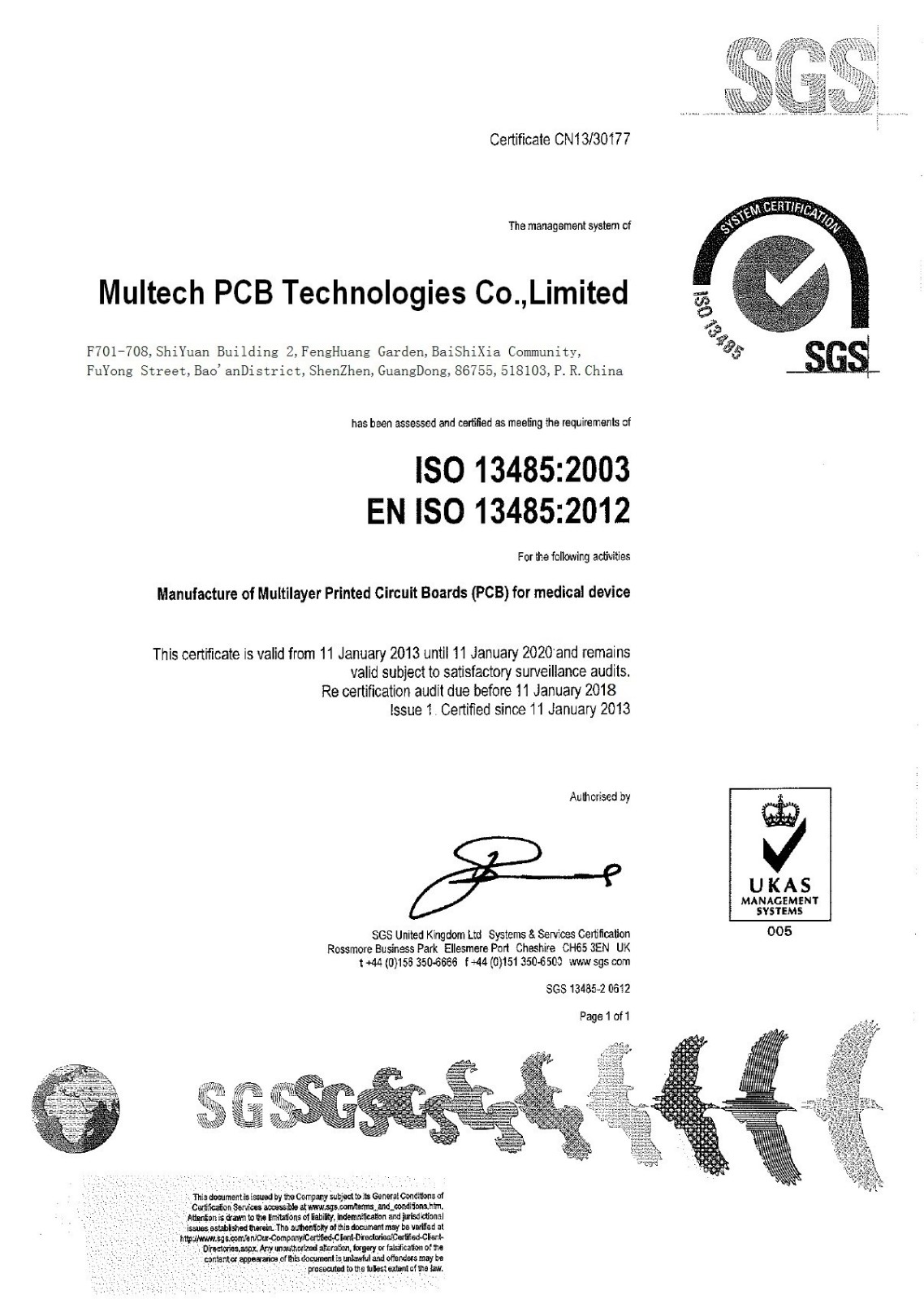
ISO 13485
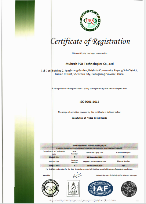
ISO 9001
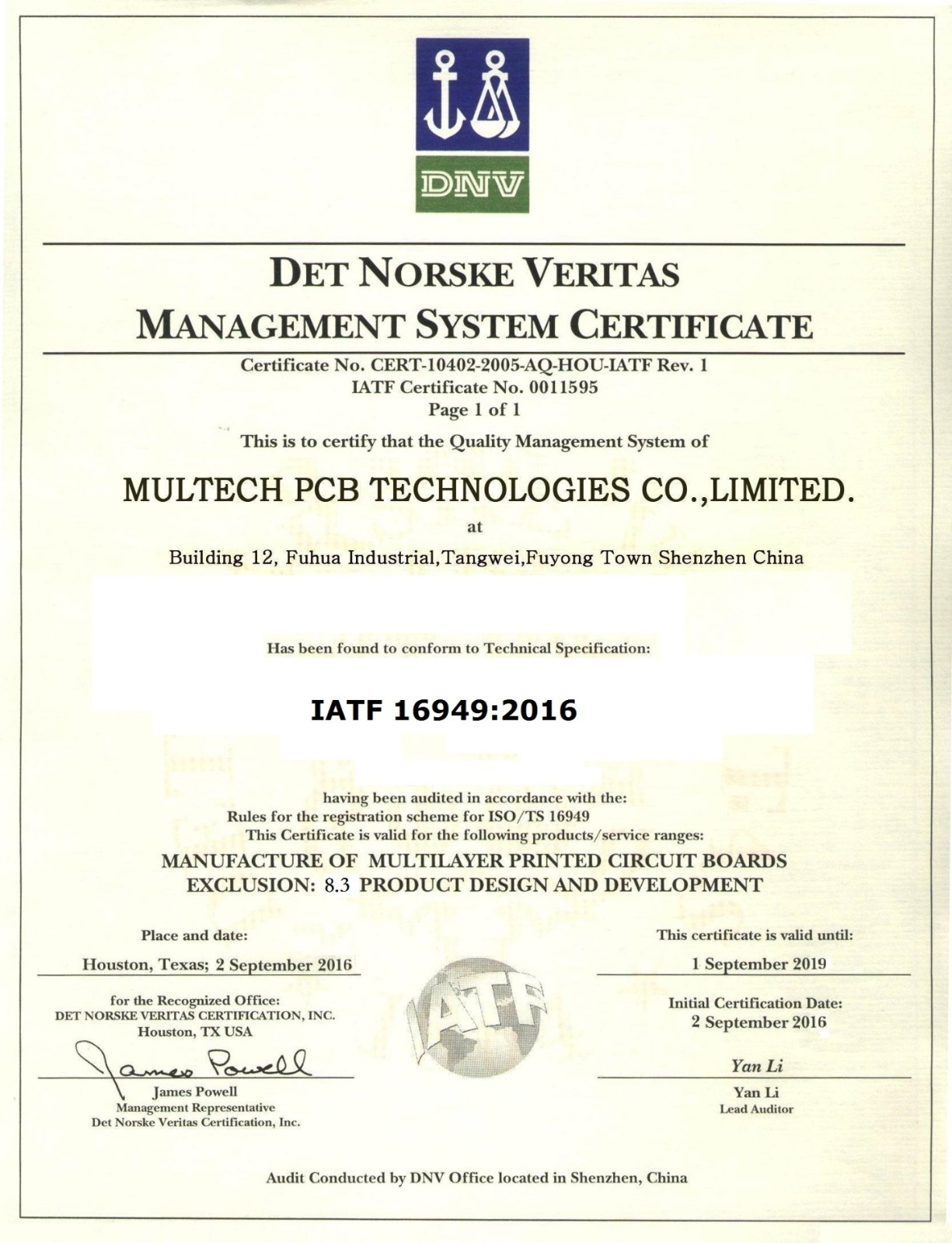
IATF 16949
ISO 14001
Manufacturing Process:

Product Quality Testing
· Material verification – Thermal conductivity (laser flash method), CTE (dilatometer), porosity (microscopy).
· Metallization adhesion – Peel strength ≥1.5 N/mm for thick‑film; tape test for thin‑film (no lift‑off).
· Surface finish thickness – XRF for Au/Ni/Ag (e.g., 0.3–0.5μm Au for bondable pads).
· Line resolution inspection – High‑magnification optical or SEM for trace/space (50μm target).
· Thermal shock test – -55°C ↔ +150°C, 200 cycles, no delamination or cracks.
· Insulation resistance – >10¹² Ω at 500V DC (AlN).
· Solderability – Wetting balance per IPC-J-STD-003 (for thick‑film Ag/ENIG).
· Electrical testing – 100% continuity and isolation for ceramic circuits.
Quality Control
· Certifications: ISO9001:2015, IATF16949 (automotive optional), AS9100D (aerospace on request), RoHS.
· Process controls: Real‑time monitoring of sputtering deposition rate, firing temperature profile, and photolithography alignment.
· Traceability: Each ceramic batch is recorded (lot number, thickness, sintering curve).
· Inspection: 100% AOI for thin‑film pattern, 100% visual for thick‑film defects (pinholes, bridging).
· Reliability lab: In‑house thermal cycling, high‑temperature storage (200°C), and humidity (85°C/85%RH) chambers.
Pre-sale and After-sale Service
· Pre-sale
· Free DFM review for ceramic layout (thin‑film vs. thick‑film process selection).
· Thermal simulation and CTE matching advice.
· Small quantity prototyping (≤5 pcs) within 7–10 working days.
· After-sale
· 12‑month warranty against material defects or metallization failure.
· 24‑hour technical support (including failure analysis).
· Full test report (including thermal, electrical, adhesion...) provided along with each shipment.
FAQ
Q1: What is the difference between thin‑film and thick‑film ceramic PCB?
A: Thin‑film uses sputtering and photolithography for fine trace (≥50μm) with tight tolerances; thick‑film uses screen printing and firing for lower resolution (≥150μm) but lower cost for simple circuits. We can provide both of the above.
Q2: Which ceramic material should I choose: Al₂O₃ or AlN?
A: Al₂O₃ is cost‑effective and apply for moderate power (24–30 W/m·K). AlN is for high power (>170 W/m·K) and CTE matching to silicon. Choose AlN for high‑power laser diodes or high‑brightness LED arrays.
Q3: Can you drill through‑holes in ceramic material?
A: Yes, we use UV laser drilling technology for vias diameter as small as 0.1mm and punched/ultrasonic holes for larger diameters (≥0.3mm). Thick‑film can fill vias with conductive paste.
Q4: What surface finish is best for wire bonding?
A: Bondable gold (≥0.5μm Au over Ni) or soft gold (≥1.0μm). Our ENIG can be customized for Au thickness.
Q5: Is ceramic PCB suitable for flex applications?
A: No, ceramic is rigid and brittle. It is not flexible. For flex‑rigid, use FR4 + ceramic hybrid modules.
Q6: Can you manufacture large‑size ceramic panels?
A: Maximum typical size is 120mm×120mm for AlN and 150mm×150mm for Al₂O₃ due to firing shrinkage. Larger sizes may be available for via post‑polishing.
Q7: What is the lead time for prototype ceramic PCBs?
A: Thin‑film prototype for 7–10 working days. Thick‑film prototype for 10–12 working days (including the paste firing cycles).
Q8: Can you provide metallized edge or wrap‑around conductors?
A: Yes, we can provide solderable edge metallization for surface mount or castellated holes.
Q9:What’s your minimum order quantity (MOQ)?
A:Our MOQ is 1 piece. We support prototype orders, small-batch trials, as well as medium and high-volume mass production to meet diverse R&D and production needs.
Q10: What are the transportation methods used by your company?
A: Air transport, sea transport, rail transport, DHL, FEDEX, UPS, TNT and certain designated freight forwarders for customer's needs.
Q11: What is your usual method of payment?
A: We usually use bank transfers and Paypal for receiving payments.
After-sales service:
At Multech we believe a good PCB is just the start of the collaboration. What really makes clients walk with us for 20 years is our accountability for problems, our expertise with every technical consultation.
- Quality Assurance: 100% tested. Any defect we will reproduce free.
- Technical Support: Lifetime access to our engineering team for consultation including review of design files, guidance on documentation, design recommendations and DFM (Design for Manufacturing) advice.
- Fast Response: All complaints will be acknowledged within 48 hours.
- Long-term Partnership:Professional account management services for large order volumes.