

Thermally Isolated Copper Substrate
Thermally Isolated Copper Substrate
1.6mm thickness
8/8mil line width/space
ENIG(1U”)
2oz finished
100% AOI Test
ISO.9001/CQC/ISO.TS16949/ROHS
Application:Consumer/home/network
- Multech
- China
- 7-10 days
- 88000sqm/month
Product Description:
The Thermally Isolated Copper Substrate is a single-layer circuit board designed using thermoelectric separation technology. The circuit path and thermal path are physically isolated on a solid copper base, achieving ultra-low thermal resistance. Surface finish is immersion gold (ENIG) at 1 microinch (1u″). Total board thickness is 1.6mm with finished copper thickness of 2oz (70um). This construction is ideal for high-brightness LEDs, laser modules, and RF power amplifiers where heat must be removed directly without interfering with electrical signals.
Product Specifications: Thermally Isolated Copper Substrate
Parameter Category | Specification |
|---|---|
Board Thickness | 1.6mm |
PCB Type | Base Material Copper (C1100/C1020, Cu≥99.9%) |
Line Width/Space | 8/8mil |
Surface Finish | ENIG (1U”) |
Finished Copper Thickness | 2oz |
Testing Standard | 100% AOI Test |
Certifications | ISO 9001 / CQC / ISO TS16949 / ROHS |
Applications | Consumer Electronics / Telecom Equipment / Network Devices / Automotive Electronics |
Product Advantages:
· True thermoelectric separation – Thermal and electrical paths are physically isolated → no electrical noise coupling into heat sink, maximum heat dissipation.
· Ultra-low thermal resistance – Direct copper-to-thermal pad eliminates insulating dielectric layer under thermal vias, achieving <1.0 K/W.
· Heavy copper (2oz) – Low resistive loss for high-current driving (up to 10A+) with minimal temperature rise.
· ENIG finish (1u″ gold) – Excellent wire-bonding capability (for LED chip attachment), flat surface for solder reflow, and long shelf life (>12 months).
· 1.6mm rigid copper base – High mechanical stability and easy mounting with screws or clamps.
· RoHS compliant – Lead-free and compatible with standard SMT assembly.
Company Profile:
Founded in 1997, Multech PCB is a leading manufacturer of high-end printed circuit boards in China with nearly 30 years of industry experience. Founded by senior PCB experts, the company's headquartered locates in Qianhai, Shenzhen, with its production base is located in Huizhou. It covers a workshop area of over 20,000 square meters and is equipped with multiple modern automated production lines, with an annual output exceeding 2 million square meters, capable of efficiently handling prototype, medium and high volume orders.
Boasting a professional R&D team of more than 60 members, the company focuses on technological innovation, specializing in high-density multilayer boards, HDI, backplane PCBs, high-frequency boards, metal core PCBs, flexible and rigid-flex PCBs and other special PCBs. 80% of its products are exported to Europe, the United States, Japan and the Asia-Pacific region, widely used in high-tech industries such as telecommunications, industrial control, medical treatment, automotive and aerospace.
The company has passed international authoritative certifications including ISO9001, ISO14001, UL, RoHS and IATF16949, with fully compliant production processes and 100% full inspection before shipment to ensure stable and reliable quality. It has long provided one-stop PCB+PCBA solutions for global well-known enterprises, winning the trust of customers at home and abroad with high quality, cost-effectiveness and prompt delivery.
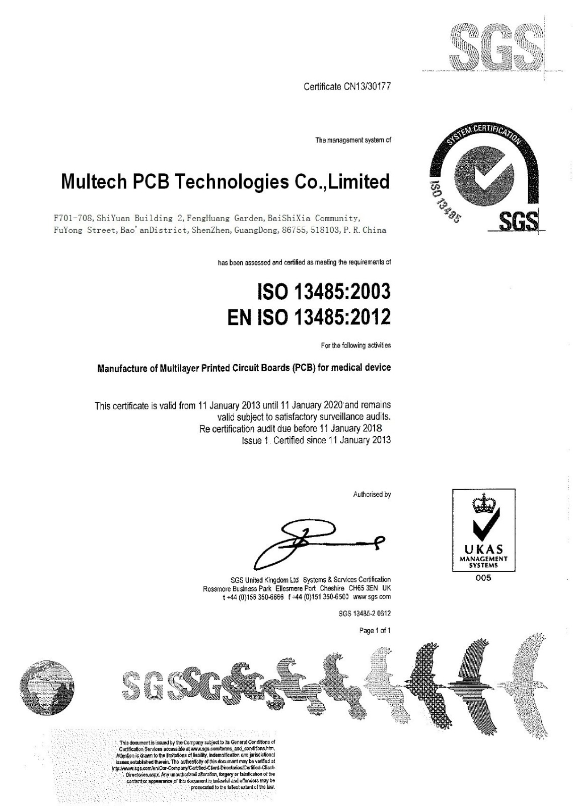
ISO 13485
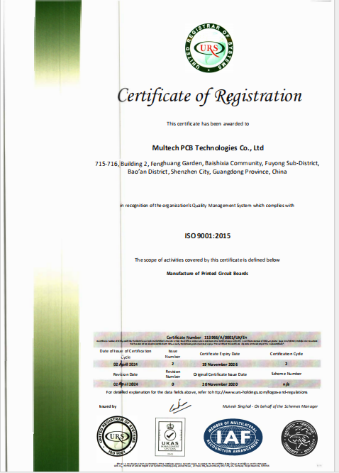
ISO 9001
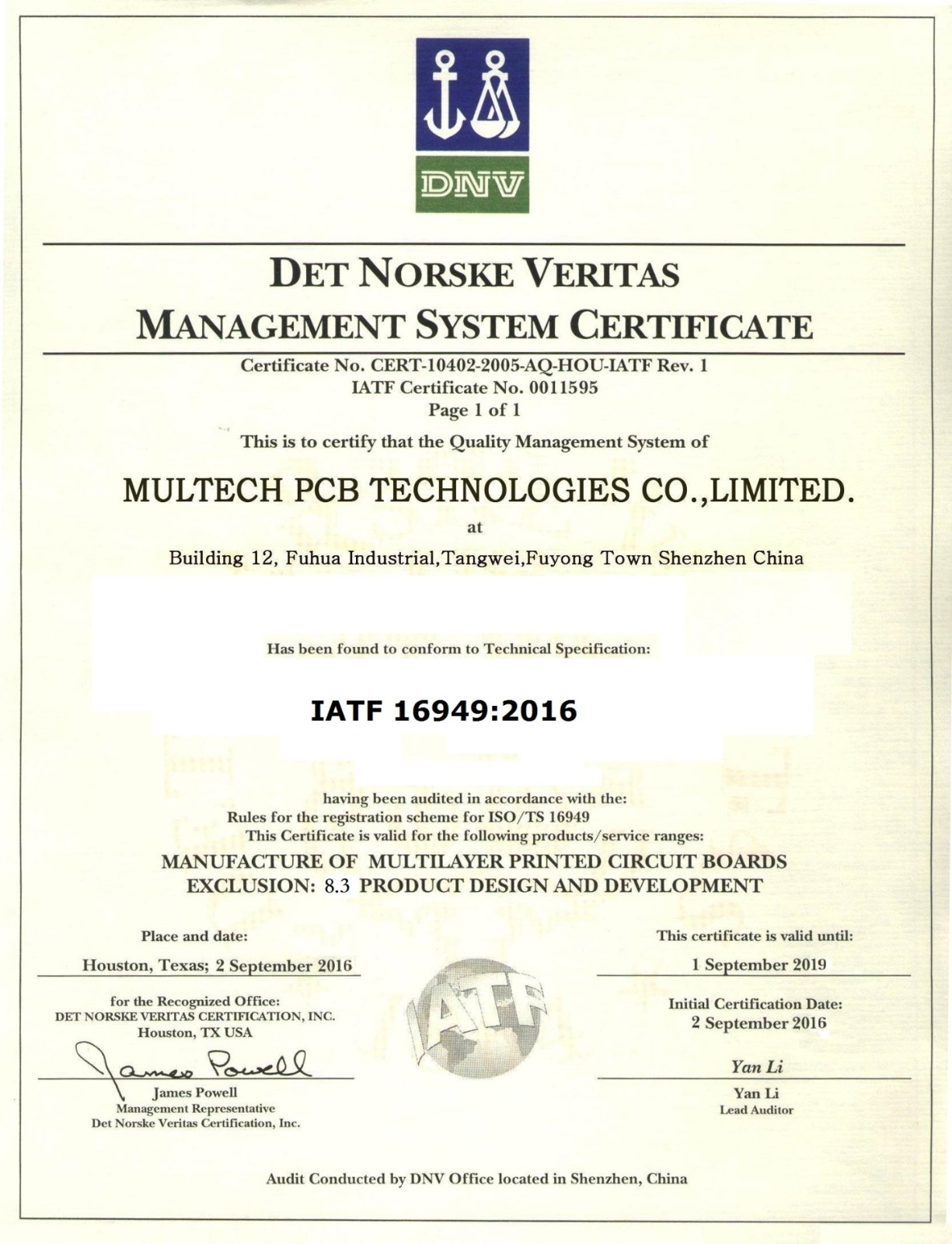
IATF 16949
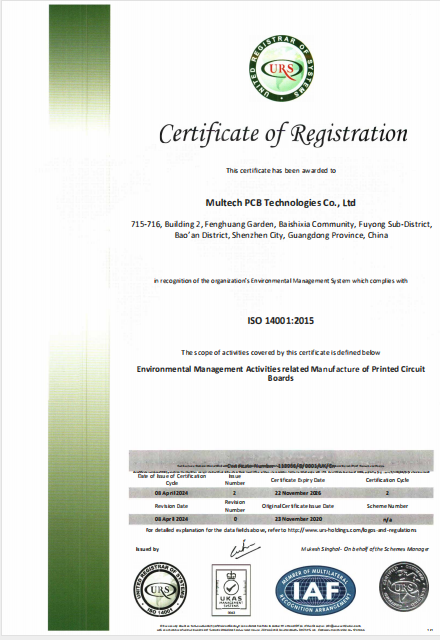
ISO 14001
Manufacturing Process:

Product Quality Testing
· Gold thickness – X-ray fluorescence (XRF) 100% measurement (1u″ ±0.2u″).
· Nickel thickness – 120–200u″, cross-section verification.
· Thermal resistance (Rth) – Tested with thermal transient tester (e.g., T3Ster) per JEDEC standards.
· Thermal isolation voltage – Dielectric withstand test between circuit pads and copper base (≥1.5kV DC).
· Peel strength – ≥1.2 N/mm for dielectric layer under circuit traces.
· Solderability – Wetting balance per IPC-J-STD-003.
· Thermal shock – -40°C ↔ +125°C, 100 cycles, no delamination or open circuit.
· Flatness/warpage – ≤0.5% of board diagonal for 1.6mm copper substrate.
Quality Control
· Certifications: ISO9001:2015, IATF16949, UL (copper base recognition).
· Process controls: SPC for etching 2oz copper, lamination of selective dielectric (only under circuit traces), ENIG plating.
· Traceability: Each copper plate and ENIG bath batch has unique lot number.
· Inspection: 100% AOI for circuit pattern, 100% electrical & thermal resistance test for key thermal pads.
· Reliability lab: In-house thermal cycling, humidity (85°C/85%RH, 168h), and insulation resistance (>100MΩ).
FAQ:
Q1: What exactly is “thermoelectric separation” on a copper substrate?
A: It means the electrical circuit traces are on a dielectric layer while the thermal pads (for component backside) are directly on exposed copper, creating separate paths – heat conducts directly to the base without passing through isolating material.
Q2: Why is ENIG gold only 1u″? Is that enough for soldering?
A: 1u″ gold is sufficient for wire bonding and light soldering (once). For repeated soldering or aggressive environments, we recommend 2-3u″. We precisely control 1u″ for fine-pitch bonding applications.
Q3: What is the thermal resistance value you guarantee?
A: For a standard 10×10mm thermal pad, Rth is <1.0 K/W. Contact us for your specific pad area.
Q4: Can I use this board for both high current and high voltage isolation?
A: Yes, the dielectric layer under circuit traces withstands >1.5kV DC isolation between circuit and copper base. However, thermal pads are electrically connected to the copper base (non-isolated).
Q5: How do you ensure no short circuit between circuit and thermal pads?
A: We design a physical gap (≥0.2mm) between the dielectric-covered circuit area and exposed copper thermal pads. 100% electrical testing verifies isolation.
Q6: What is the maximum LED power this substrate can handle?
A: For a single 5mm×5mm LED chip, it can handle up to 20W thermal dissipation with proper heatsink mounting. Consult our engineers for system-level design.
Q7: Is the 2oz finished copper thickness measured after plating?
A: Yes, finished copper includes starting copper foil + plated copper. Cross-section verifies 2oz (70um) minimum on traces.
Q8:What’s your minimum order quantity (MOQ)?
A:Our MOQ is 1 piece. We support prototype orders, small-batch trials, as well as medium and high-volume mass production to meet diverse R&D and production needs.
Q9: What are the transportation methods used by your company?
A: Air transport, sea transport, rail transport, DHL, FEDEX, UPS, TNT and certain designated freight forwarders for customer's needs.
Q10: What is your usual method of payment?
A: We usually use bank transfers and Paypal for receiving payments.
After-sales service:
At Multech, we believe a good PCB is just the beginning of the collaboration. What truly makes clients choose to walk with us for 20 years is our expertise with every technical consultation when problems arise.
- Quality Assurance:100% tested. Free re-production for any defects.
- Technical Support: Lifetime access to our engineering team for consultation, including design file review, documentation guidance, design recommendations, and DFM (Design for Manufacturing) advice.
- Rapid Response: Initial feedback within 48 hours for any complaints.
- Long-Term Partnership:Professional account management services for high-volume orders.


